Hanson Liu
About me

Hi! I'm Hanson ^_^ 👋
I'm currently an M.S. student in the Electronic Circuits & Systems department at UC San Diego. My current interests are High-Speed Wireline and RFIC design.
In my free time, I love listening to and exploring new music, reading (you should check out my Goodreads hehe ;3), playing guitar, arranging flowers, and skiing!
Please feel free to check out all my projects!
Work experience
RFIC Design Intern

Currently working on improving the power-handling of high-power, broad-market RF switches.
I also do some lab work, where I characterized in-development RF switches for power derating, IIP3, S-parameters, and thermal performance.
Applications Engineering Intern

Worked for the High Power (HP) applications team, where I performed PSRR characterization and designed an AC Ripple Injector PCB.
Teaching Assistant

During my time at UCSD, I realized I also had a passion for teaching. I'll always be thankful to my first really GREAT TA, who inspired me to continue to create a strong and supportive learning environment for others here in the UCSD ECE department.
As a teaching assistant, I held office hours, discussion sections, review bootcamps, and circuit lab sessions. I served as a mentor across five different courses:
- ECE 35 — Introduction to Analog Design · Prof. Curt Schurgers & Prof. Rajeev Sahay
- ECE 65 — Components and Circuits Laboratory · Prof. Saharnaz Baghdadchi
- ECE 100 — Linear Electronic Systems · Prof. Tzu-Chien Hsueh
- ECE 102 — Introduction to Active Circuit Design · Prof. Tzu-Chien Hsueh
- ECE 163 — Electronic Circuits and Systems · Prof. Tzu-Chien Hsueh
If you want, check out my SET reviews!
Engineering Chair & Tech Lead

Served as a leader and mentor to develop educational discrete circuits for workshops/showcases that teach introductory hardware and software skills to college students and K-12. Led and created:
Integrated circuit projects
My proudest moments here at UCSD!
I hope you enjoy checking out these projects as much as I did making them!
A Unit-Via Based Delta-Length SAR ADC Design & Tapeout
My MAGNUM OPUS! All the blood, sweat, and tears my partner and I poured into this! All 5 years here at UCSD, has led up to this very moment!
View project →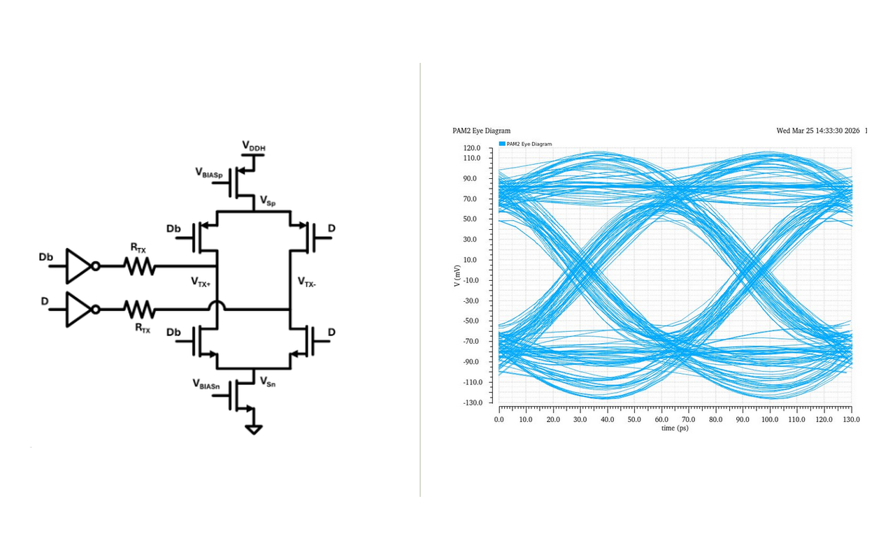
PAM2 / PAM4 Voltage-Mode Hybrid Transmitter
I along with my partners designed a voltage-mode driver with auxiliary push/pull current-mode swing enhancement! We did both PAM2 and PAM4, with max data rates of 18Gbps and 20Gbps respectively!
View project →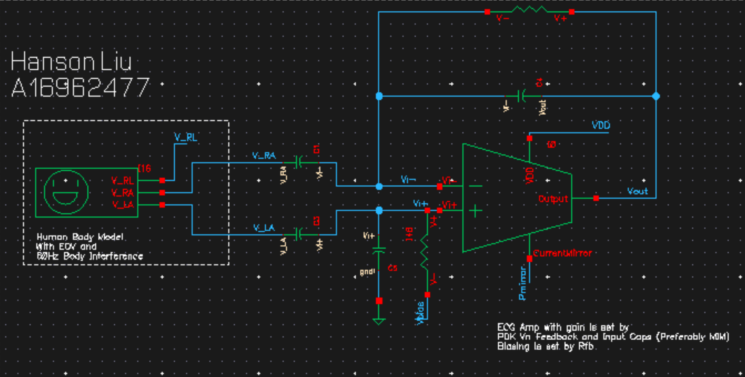
Ultra Low-Power Electro-Cardiogram Instrumentation Amplifier
Designed a super optimized ECG amplifier with just two op-amps! Received top-score for design performance and report. Come check out how I did it.
View project →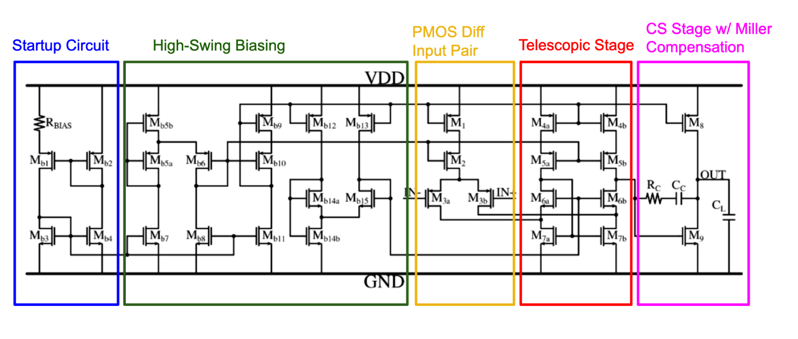
Folded-Cascode OTA
A very heavily optimized design, seeking to maximize gain while still meeting bandwidth specifications. I along with my partner got to present our approach and design to apple!
View project →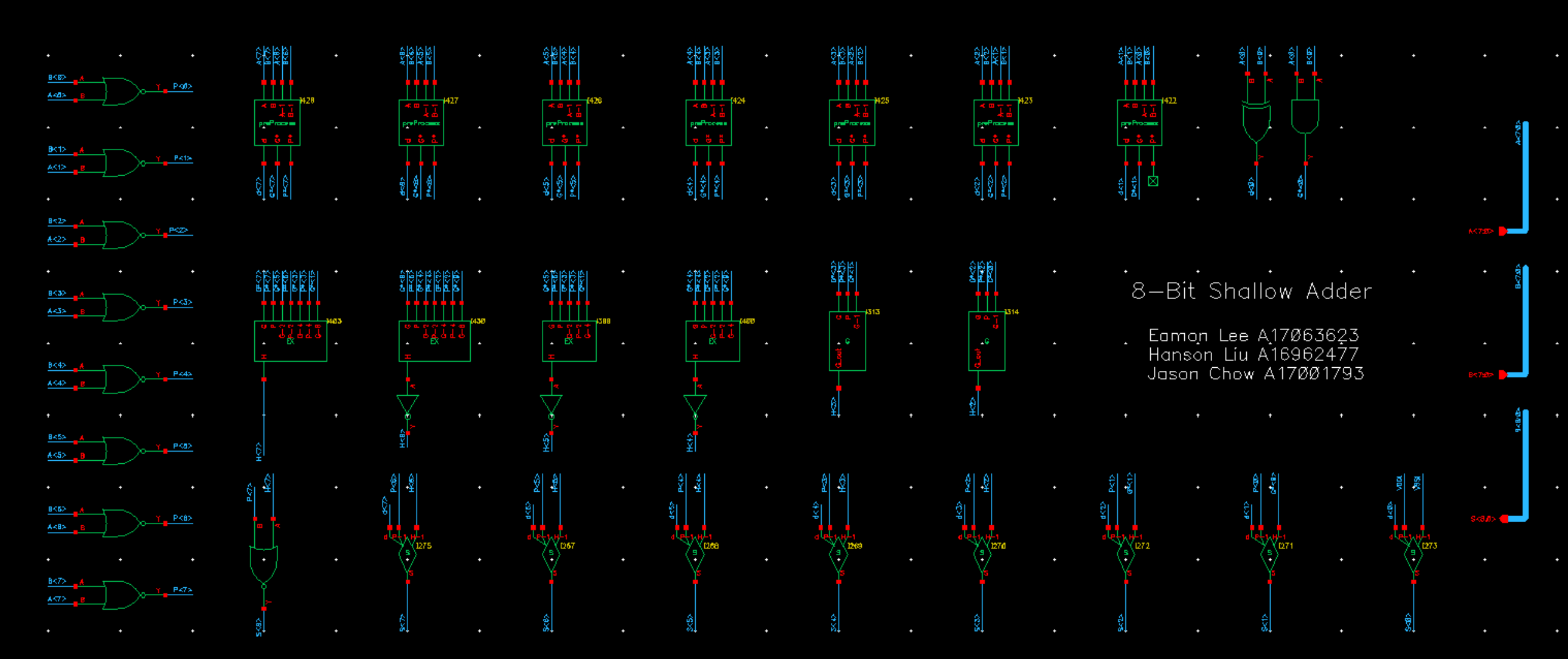
8-Bit Carry-Less Adder
A 1.1V Ladner Fischer Ling Carry Adder! Was able to clock up to 4.8 GHz.
View project →Hardware projects
Discrete Builds!
A lot of where my passion for engineering began!
AC Ripple-Injection Lab Board
An AC-ripple injector for characterizing how well a power-regulator rejects incoming power-supply ripple (PSRR). Based on Analog Devices AN-159.
View project →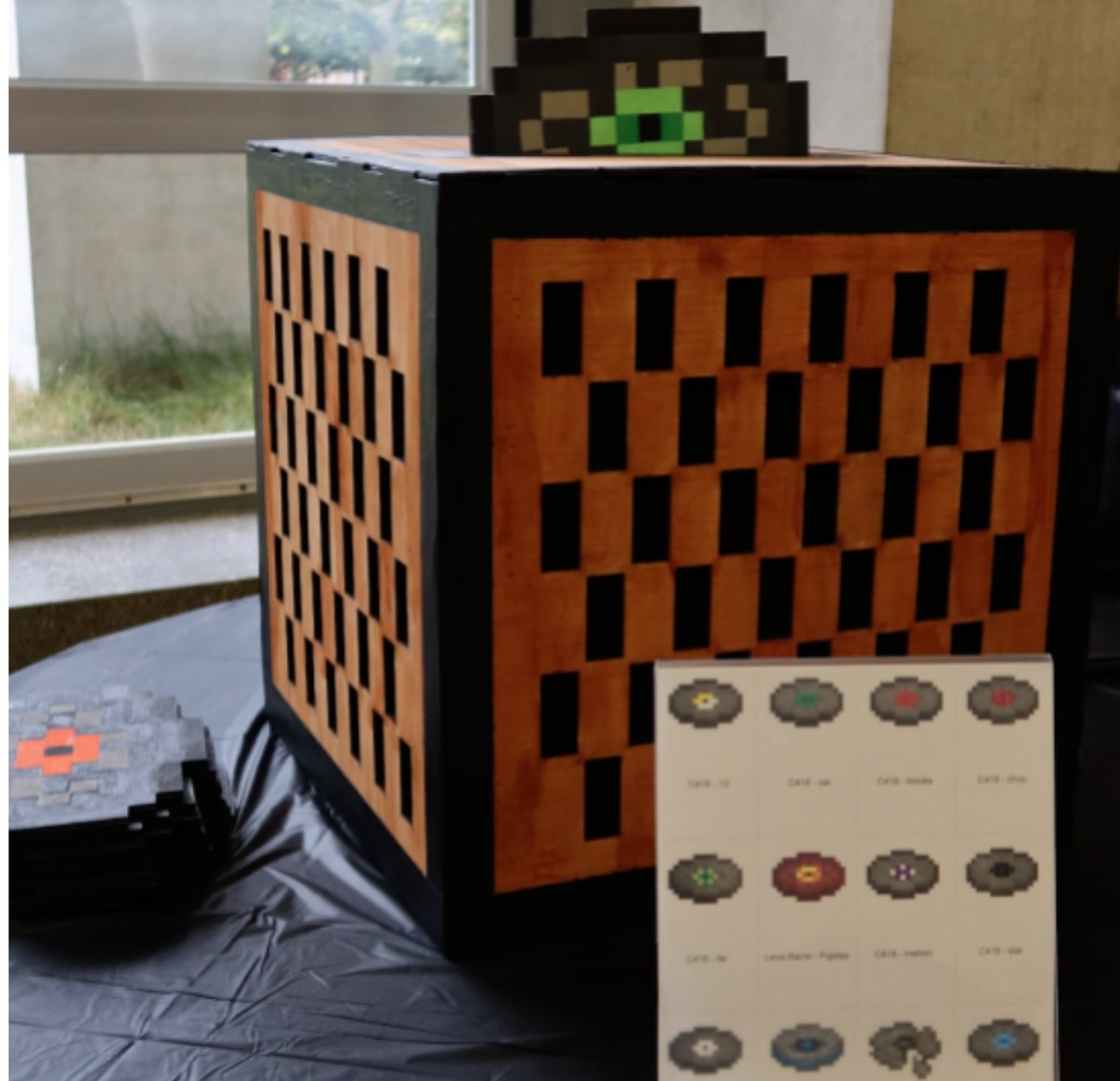
A Fully Functional Minecraft Jukebox
A life-size, working build of the MC jukebox, implemented with RFID!
View project →Discrete Delay Guitar Pedal
My current project! Trying to build a discrete delay guitar pedal built around the PT2399 delay chip. Currently in progress, I'll have the full writeup up once the build is finished.
Screaming Plant
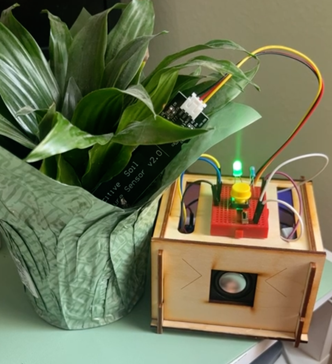
A plant that screams when its thirsty. Inspired by TikTok.
View project →Hardware project
AC Ripple-Injection Lab Board
During my time at ADI as an Applications Engineering Intern for the HP Team, along with a lot of lab work that involved power-regulator characterization, I was also tasked with the project of developing a ripple injection PCB!
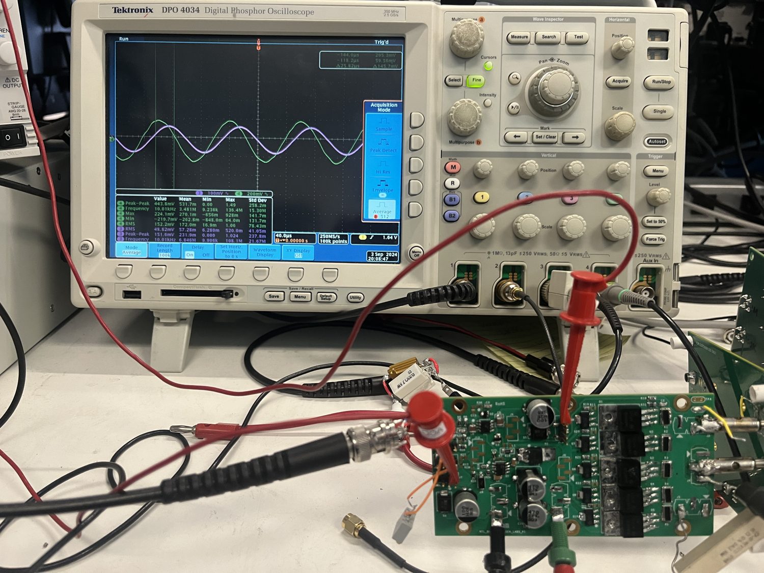
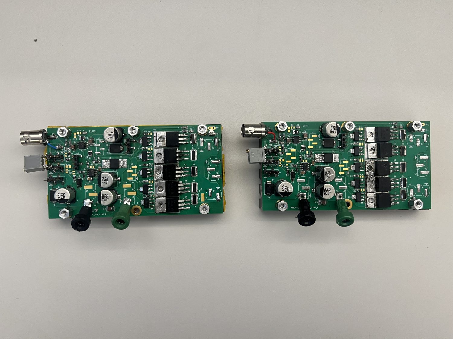
Based on Application Note AN-159, the board's goal is to inject a controlled AC ripple on top of a DC voltage, so a power-regulator's ability to reject that ripple (PSRR) can be characterized on the bench. The project entailed finding new SMD components to replace original THT copper-plate design then doing all the component routing in Cadence Allegro. The new revision was verified in LTspice with each new component's respective modeling imported to confirm it still functioned and was still closed-loop stable.
Thanks to my mentor, we were able to finish the board before my internship finished! Towards the last couple weeks of my internship, I got to personally use the board to characterize the PSRR of several ADI/LT LDOs, as well as the Silent Switcher 3 Buck Regulators, across a range of current-loading conditions.
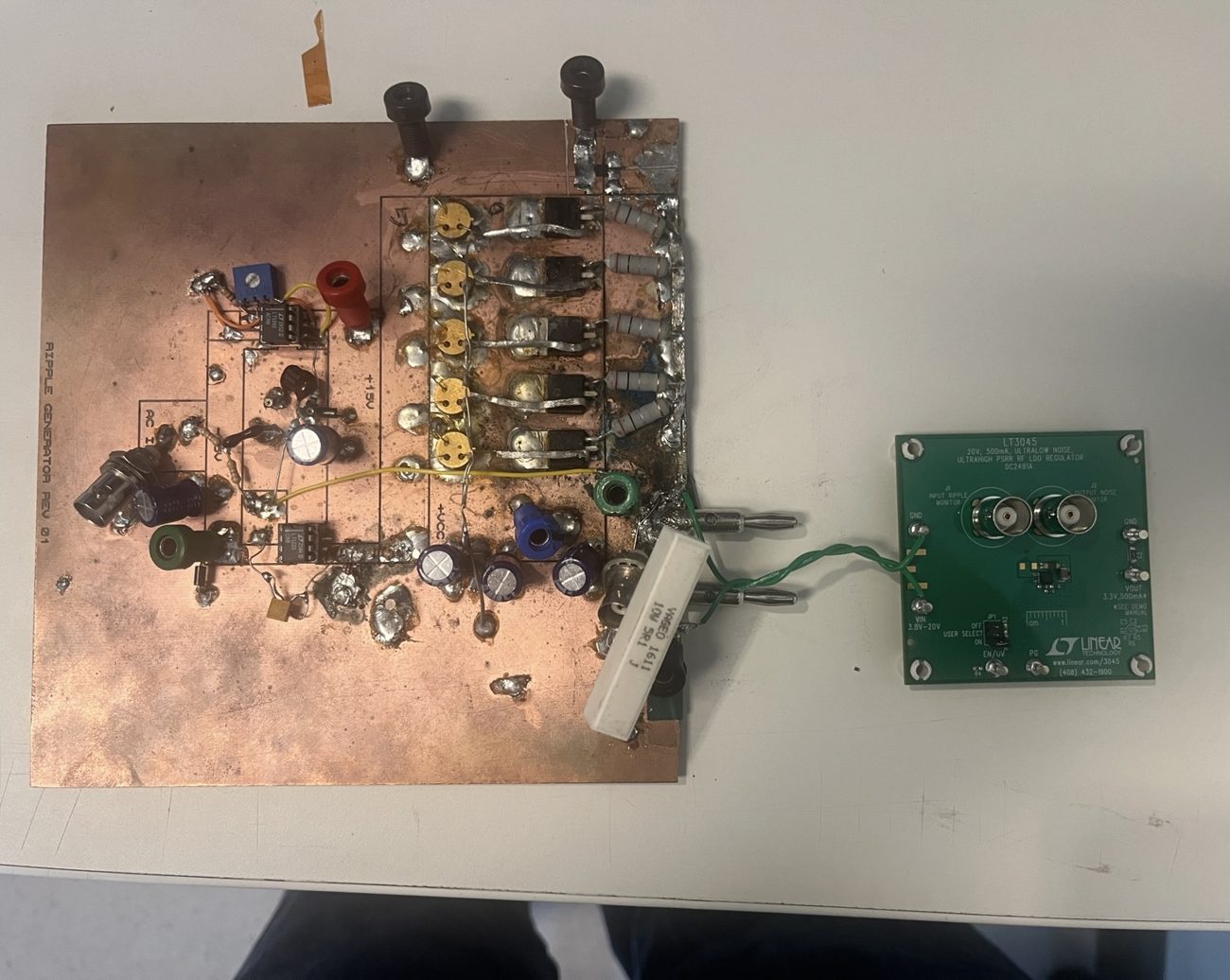
The original ripple injector, everything was built on a solid copper plate! Connections were made with cut out pads directly into the copper and components were hand soldered across the cuts
My PCB revision of the ripple injector!
New Ripple Injector in Action! The scope shows both the injected input ripple and the regulator's output ripple, the latter amplified by an off-board LNA.
Hardware project
Minecraft Jukebox
One of my favorite projects that I've led here at Project in a Box! I, along with my amazing team of technical leads, developed a fully functional life-size minecraft jukebox!
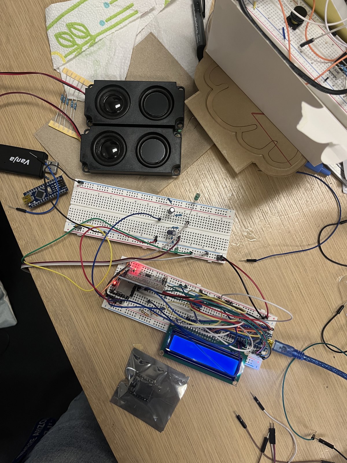
The project is fully coded in the Arduino IDE. It implements a RFID module to read RFID cards sandwiched inside the MC Jukebox discs, each card's ID maps to a specific track to be played. The music is implemented with a DFMini MP3 Player Module. After a card's ID is recognized, the DAC outputs of the MP3 module are then fed into a audio amplifier and Sallen-Key bandpass filtering signal chain, optimized for a clean listening experience!
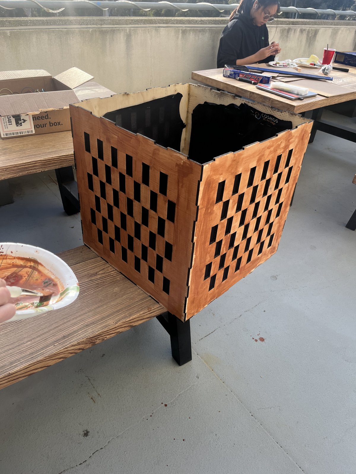
I designed the chassis of the MC jukebox in Onshape CAD, in which each wall is made of lasercut plywood to emulate the original video game's design. I personally suck at painting though, so I'd like to thank the PiB media team and my good friend Madeline Fruin for helping out with painting the jukebox and the custom discs! You guys are amazing!
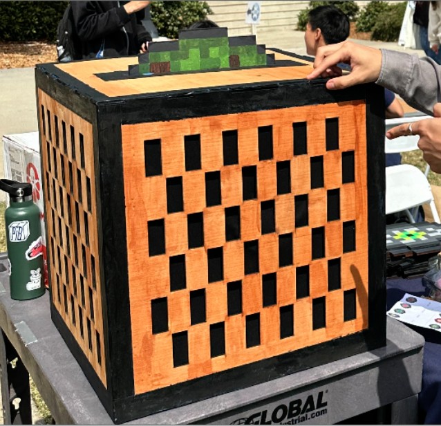
The finished Minecraft jukebox.
Demo of the jukebox.
The laser-cut plywood chassis, thanks Maddie for all the hard work!
The initial breadboard prototype on the bench.
Integrated circuit project
A Unit-Via Based Delta-Length SAR ADC
The design was completed as part of a "layout"-focused course ECE 266A, offered by Professor Drew Hall. In this course, a barebones 9-bit SAR ADC is already designed for us, and we are tasked with doing the layout in TSMC65nm using advanced layout techniques, such as common-centroid and interdigitation.
The reason why I described the class as "layout" focused, is because the option to do "extensions" is offered to students who desire a bit more challenge than others. My partner, Eamon Lee, and I, chose to do THREE EXTENSIONS! Thats right, you read it correctly, THREE!
Here are the notable changes to the original design that we took on:
- Delta-Length-based CDAC using a Unit-Via approach — based on the 2018 IEEE paper “A Compact 10-b SAR ADC With Unit-Length Capacitors and a Passive FIR Filter” by Professor Pieter Harpe.
- Monotonic Top-Plate Sampling switching scheme — based on the 2010 IEEE paper “A 10-bit 50-MS/s SAR ADC With a Monotonic Capacitor Switching Procedure” by C.-C. Liu et al.
- Bootstrapped sampling switches with Deep N-Well devices for top-plate sampling.
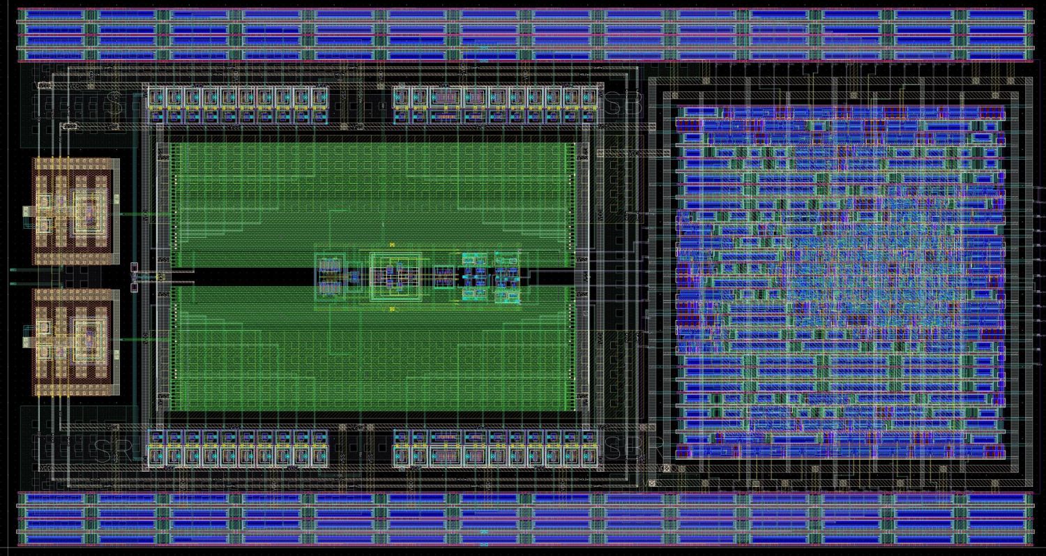
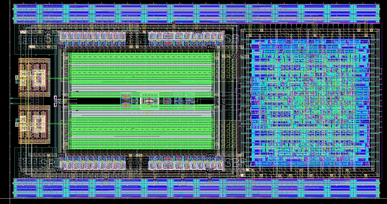
The Delta-Length DAC SAR.
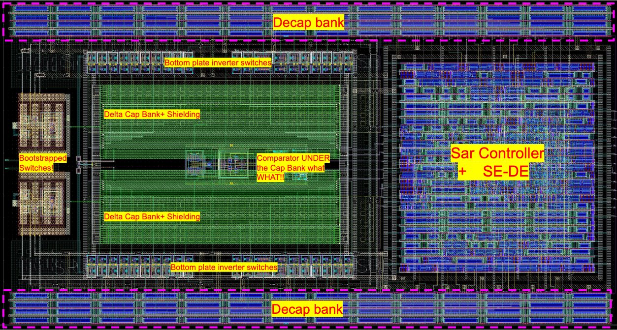
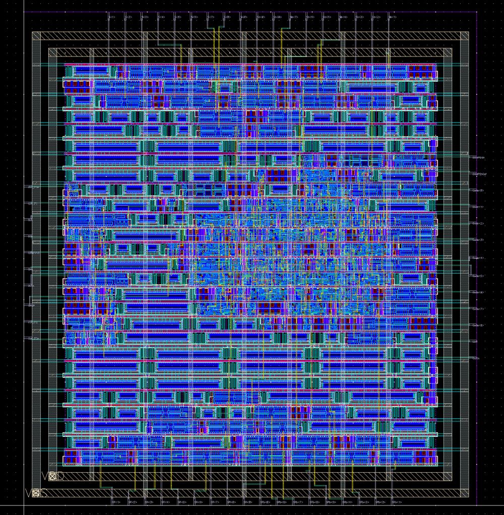
The same layout, annotated — bootstrapped switches, the delta cap bank with shielding, the comparator tucked directly under the cap bank, and the SAR controller + SE-DE.
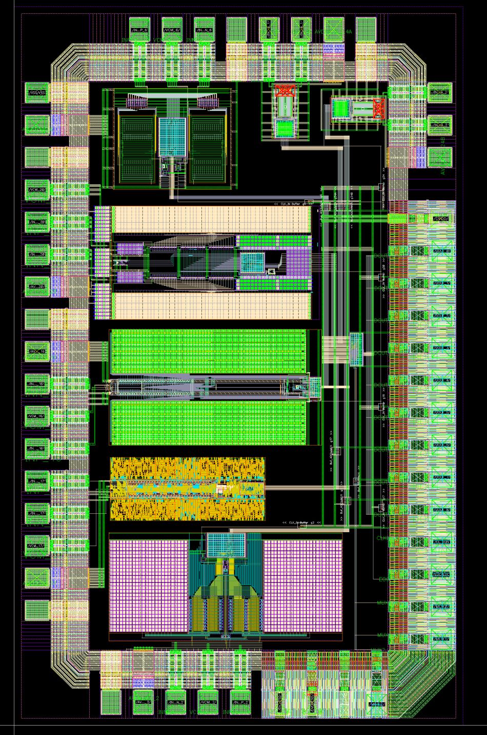
Megagroup Layout with analog/digital padring. Yes.... our design is SO SMALL, we were able to fit 2!
We were selected to present design to Apple for Design Review!
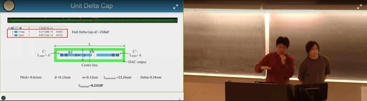
Rather than building the SAR ADC's binary weighted capacitor bank using traiditonal MOM/MIM capacitors, our SAR ADC's CDAC is built using "Delta-Caps". It is well know that we can change the capacitance of a metal strip by scaling the length. However, this does not guarantee a consistent and proportional relationship, as edge effects don't scale with length. So the premise of "Delta-Caps" can be described as this: What if we took two strips of metals, and drove one strip with positive charge, and the other strip with negative charge? From here, you can consistently account for edge effects with subtraction, and create a consistent unit capacitance by scaling the DIFFERENCE in length between the two!
However, designing a SAR ADC using these Delta-Caps comes at a nasty price. Our unit Delta-Cap had a capacitance of roughly ~280aF. Thats ATTO, not even femto! That is insanely small! Having a capacitance this small, required us to do all the additional extensions to make the Delta-Dac SAR even functional, since now we have to worry about kT/C noise...attenuation from the input capacitance of our comparator... high impedance switches driving the delta-cap strips ... it was a total nightmare!
Because of aforementioned design challenges, my partner and I sought to find ways to get the Delta-Dac SAR to just perform at a respectable level while still maintaining the incredibly compact sizing that comes with the Delta-Dac design. In the end, we were able to implement top-plate sampling, in which the outer ring laterally surrounding the delta strips were driven by boot-strapped switches for improved linearity and charge injection. Because of the incredibly small capacitances of the delta-strips, custom inverter switches were designed for each specific sized strip so optimal drive-strength can be achieved.
We also elected to implement a monotonic switching algorithm. Initially, we were concerned that common-mode (VCM) switching would connect the delta-strip capacitors to a potentially high-impedance source, degrading ADC performance. Although we later determined that VCM would be provided by a low-impedance source off-chip, we continued with monotonic switching due to its potential to reduce switching power and noise (and why not try something new!). While the resulting design achieved the lowest power consumption in the class, further reductions may have been possible with a PMOS-input comparator. Unfortunately, due to time constraints, we could not explore this by the tape-out deadline.
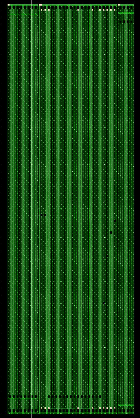
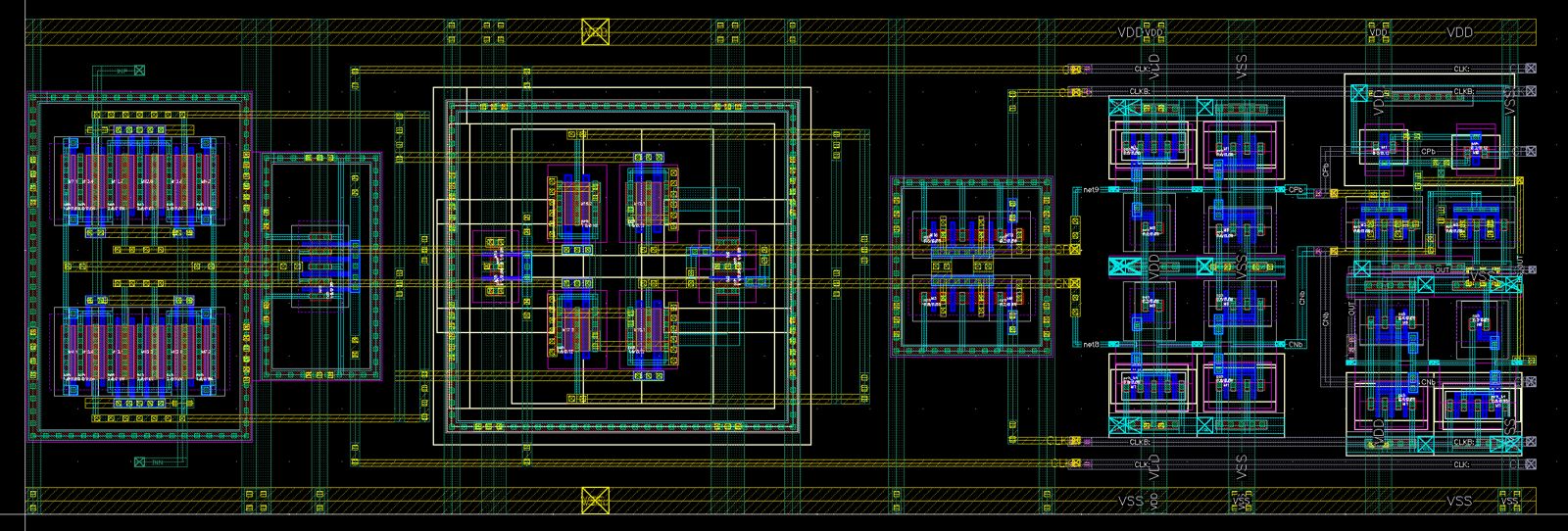
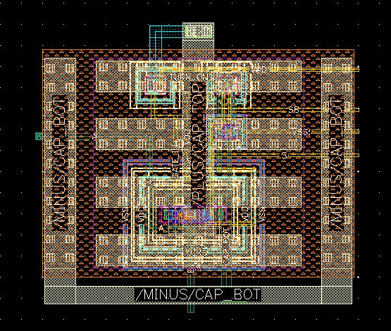
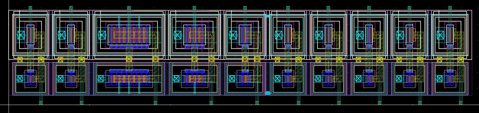
Delta-Cap bank with "dummy" Delta-Caps on left and right
Dynamic Two-Stage Comparator
Bootstrapped Switch with MIM capacitor
PNR'd Digital Controller with Monotonic Switching Algorithm and Single-Ended to Differential-Ended Converter
Inverter Switch Array Designed to Drive Delta-Dac Strips
Without further ado, here is the final performance of our SAR ADC, post extraction:
| Parameter | Value |
|---|---|
| SNDR | 49.1 dB - Pretty good for a Delta-DAC SAR! |
| Area | 143 µm × 74 µm - The smallest in the class, BY FAR! |
| Power | 120 µW - Lowest in the class! |
| Mean Comparator Offset | ~700 µV |
Integrated circuit project
PAM2 / PAM4 Voltage-Mode Hybrid Transmitter
For more information, feel free to read my report.
In this project, we were tasked with designing a high-speed wireline transmitter driving an actual noisy channel characterized by physically measured S-parameters. The design specification required, at minimum, a voltage-mode transmitter on a ≥ 1 V supply, and that the signal clear a minimum RX eye at the receiver — an eye aperture of 0.3 UI and an eye height of 20 mVppd, both at a BER of 10⁻¹² under additive noise (σ = 5 mVrms) and jitter (σ = 0.035 UIrms).
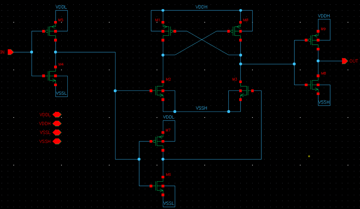
In a great pursuit to push the data-rate as HIGH as possible, my partners and I were keen on implementing some form of swing-enhancement to open our RX eye as much as we can. After some literature review, we elected to implement a hybrid transmitter design inspired from the IEEE paper “A High-Swing 45 Gb/s Hybrid Voltage and Current-Mode PAM-4 Transmitter in 28 nm CMOS FDSOI” by M. Bassi et al. , which features both a source-series terminated driver, and a auxiliary push-pull current-mode driver. To allow for even further current injection from the current-mode driver, we also designed high-speed level shifters so that our entire design can be implemented with a larger supply.
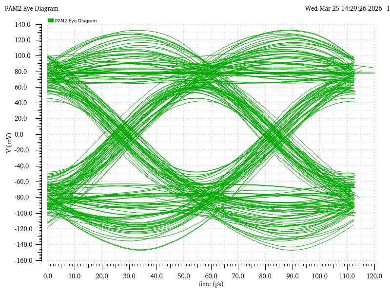
After equalization, our design was able to reach a max simulated data-rate of 18Gbps, while still clearing the RX noise and jitter spec! Yahoo!
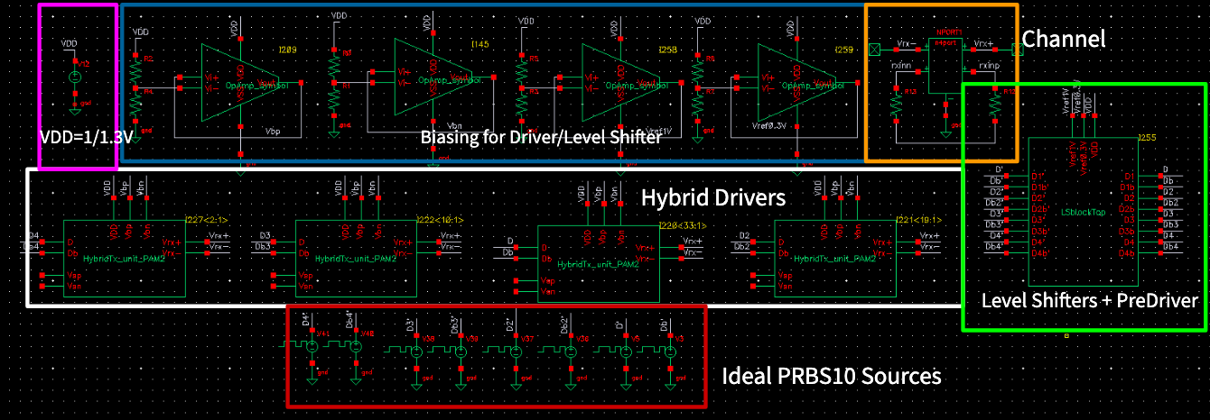
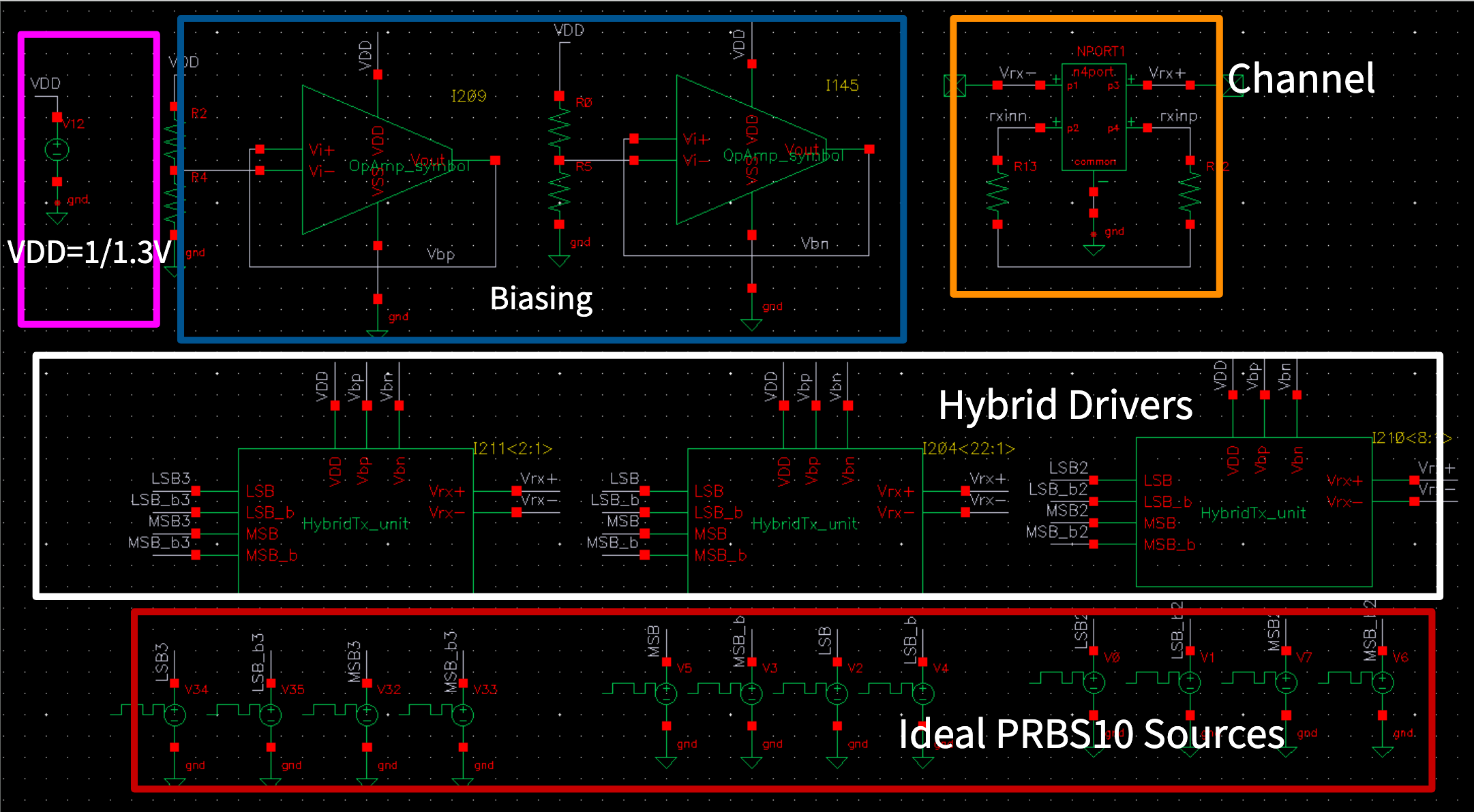
PAM-2 hybrid driver with 5-bit resolution and 4-tap FFE — top-level schematic.
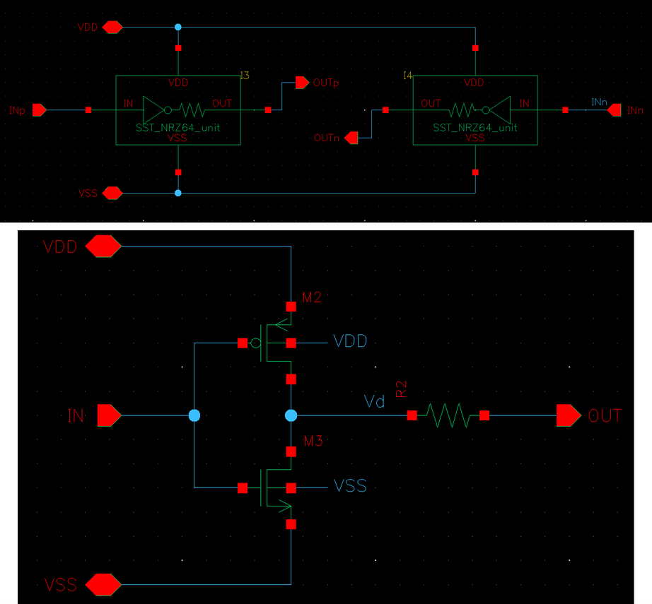
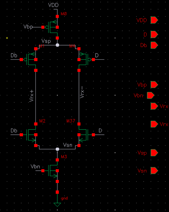
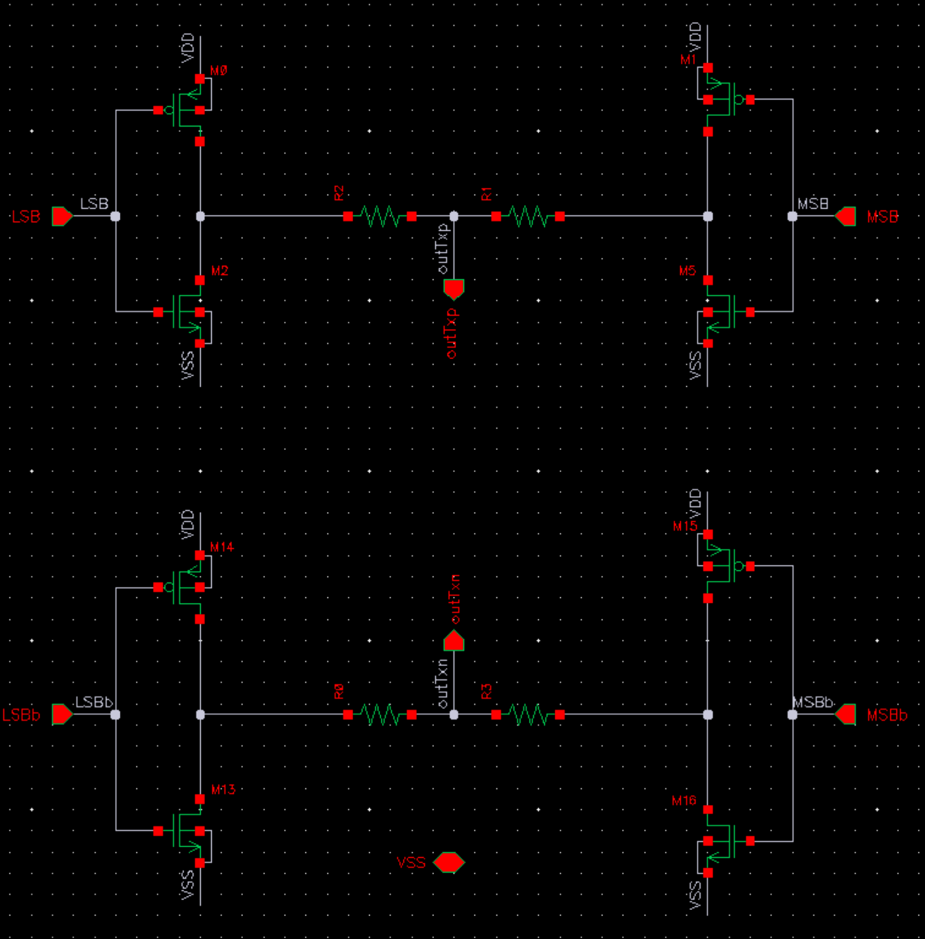
PAM2 SST (source-series-terminated) drivers.
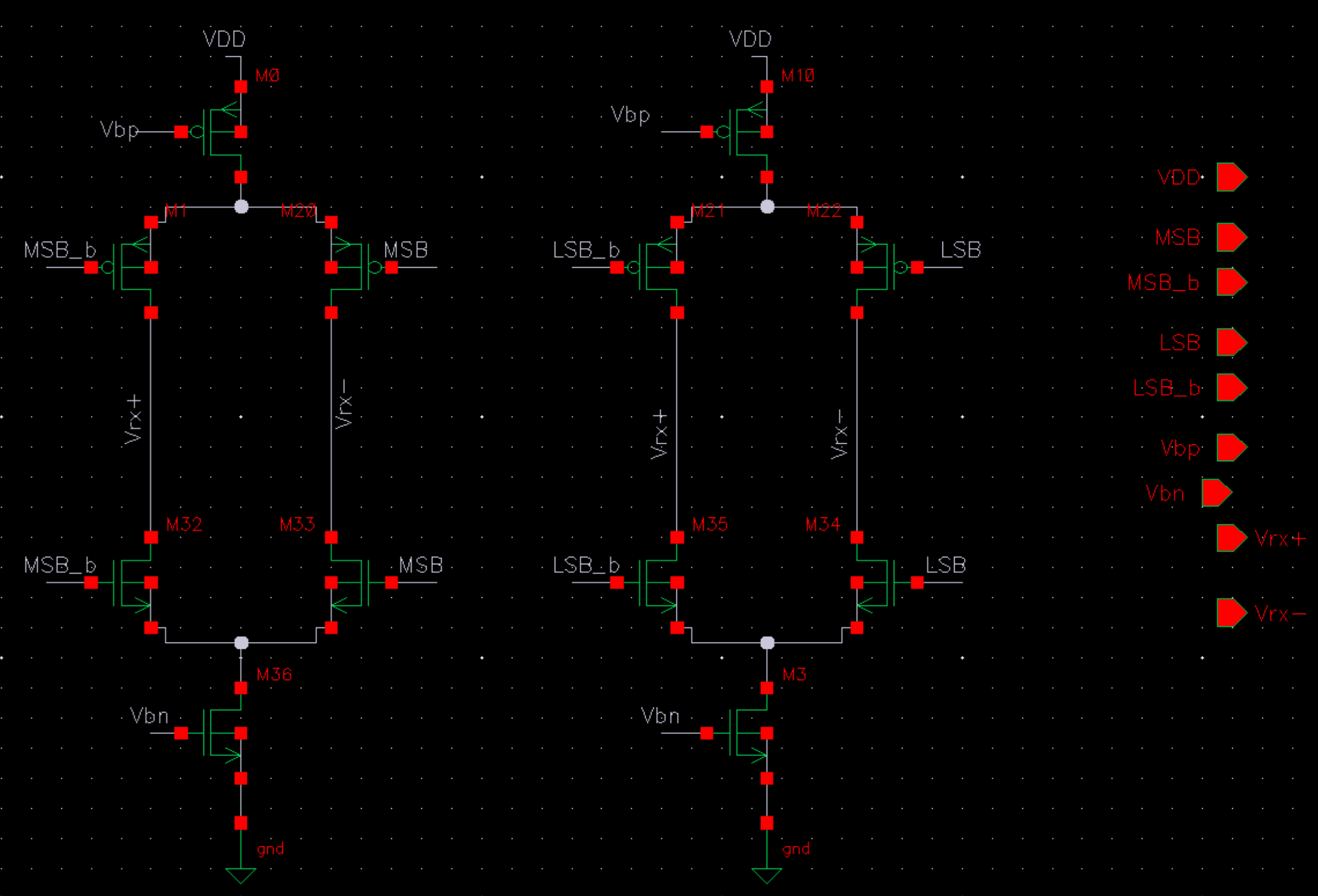
PAM2 push-pull current-mode drivers.
Type-1 high-speed level shifter.
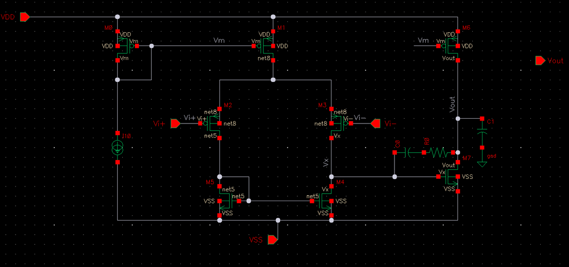
Op-amps used for replica biasing to hold the common-mode across PVT corners.
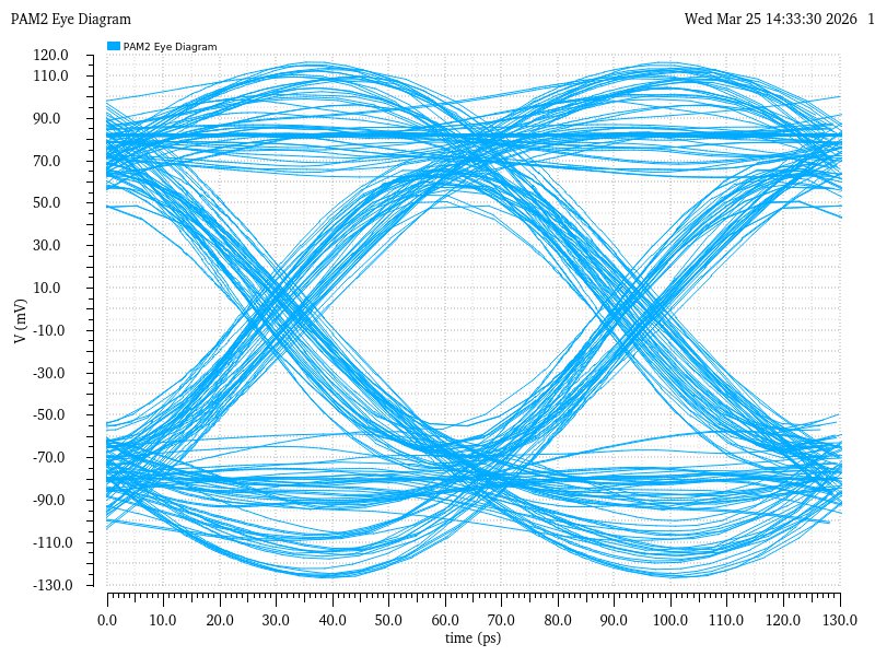
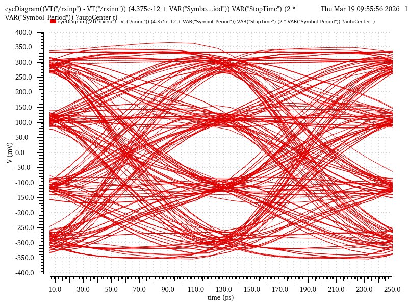
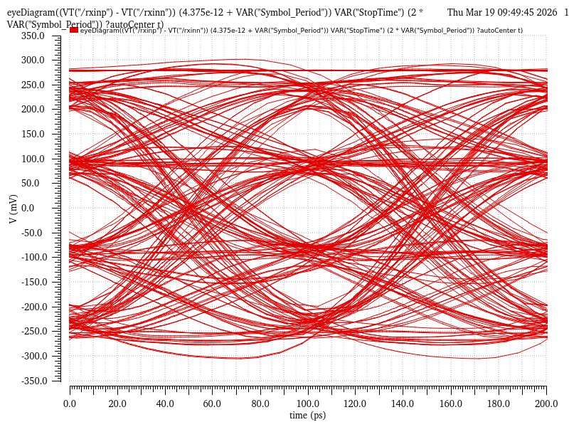
PAM2 16 Gbps eye diagram — 1 V hybrid drivers with no level shifters.
PAM2 18 Gbps eye diagram — 1.3 V hybrid driver with high-speed level shifters.
We were also able to implement the hybrid transmitter in PAM4! However, due to the nonlinear aspect of PAM4, we optimized the design to meet the provided eye height spec, as meeting the jitter spec was close to impossible. After equalization, we were able to achieve a max data-rate of 20Gbps! Holy Moly!
PAM-4 hybrid driver with 5-bit resolution and 3-tap FFE
PAM4 SST drivers.
PAM4 push-pull current-mode drivers.
PAM4 16 Gb/s eye diagram.
PAM4 20 Gb/s eye diagram
Below is the final summary of our driver's performance.
| Design | VDD | Tap Resolution / # of Taps | Max Rate | BER (w/ add. Noise) | BER (w/ add. Jitter) | Energy |
|---|---|---|---|---|---|---|
| PAM2 | 1 V | 6 bits / 4 taps | 16 Gb/s | 10−12 | 10−12 | 0.71 pJ/bit |
| PAM2 w/ HS Level Shifters | 1.3 V | 6 bits / 4 taps | 18 Gb/s | 10−12 | 10−12 | 3.5 pJ/bit |
| PAM4 | 1.3 V | 5 bits / 3 taps | 20 Gb/s | 10−12 | 3.3 × 10⁻³ | 0.65 pJ/bit |
Integrated circuit project
Ultra Low-Power ECG Instrumentation Amplifier
For more information, feel free to read my report.
The presented front-end amplifier design was developed for my final project for ECE203: Biomedical Integrated Circuits, taught by Professor Patrick Mercier. I designed an ECG amplifier that employs driven-right-leg (DRL) feedback to reduce the effects of common-mode 60Hz interference coupled in from the body. The design had to clear a baseline performance for specs relating to Mid-band Gain, CMRR, power consumption, input-referred noise, etc. Extra credit is rewarded to those who were able to push to even lower noise or lower power while keeping all other metrics iso-performance to spec.
I was able to achieve a nominal-consumption of only 667nW (yes haha funny number) and 2.7µVrms input-referred noise. My design was recognized as one of the top-performing submissions in my class, and I ended up receiving the top score in the class! Yay!
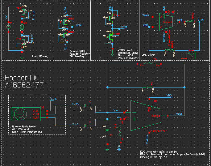
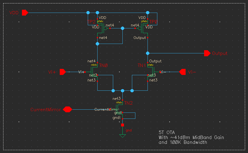
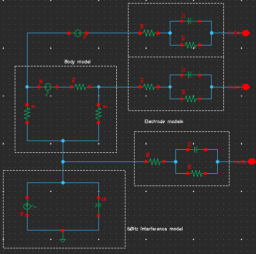
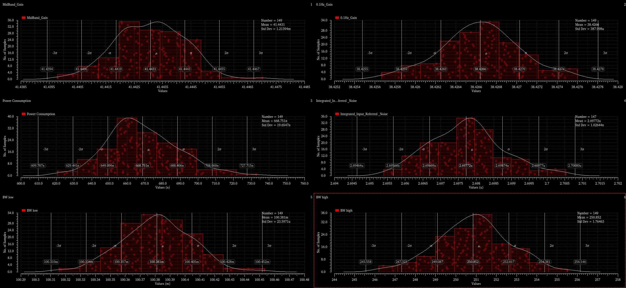
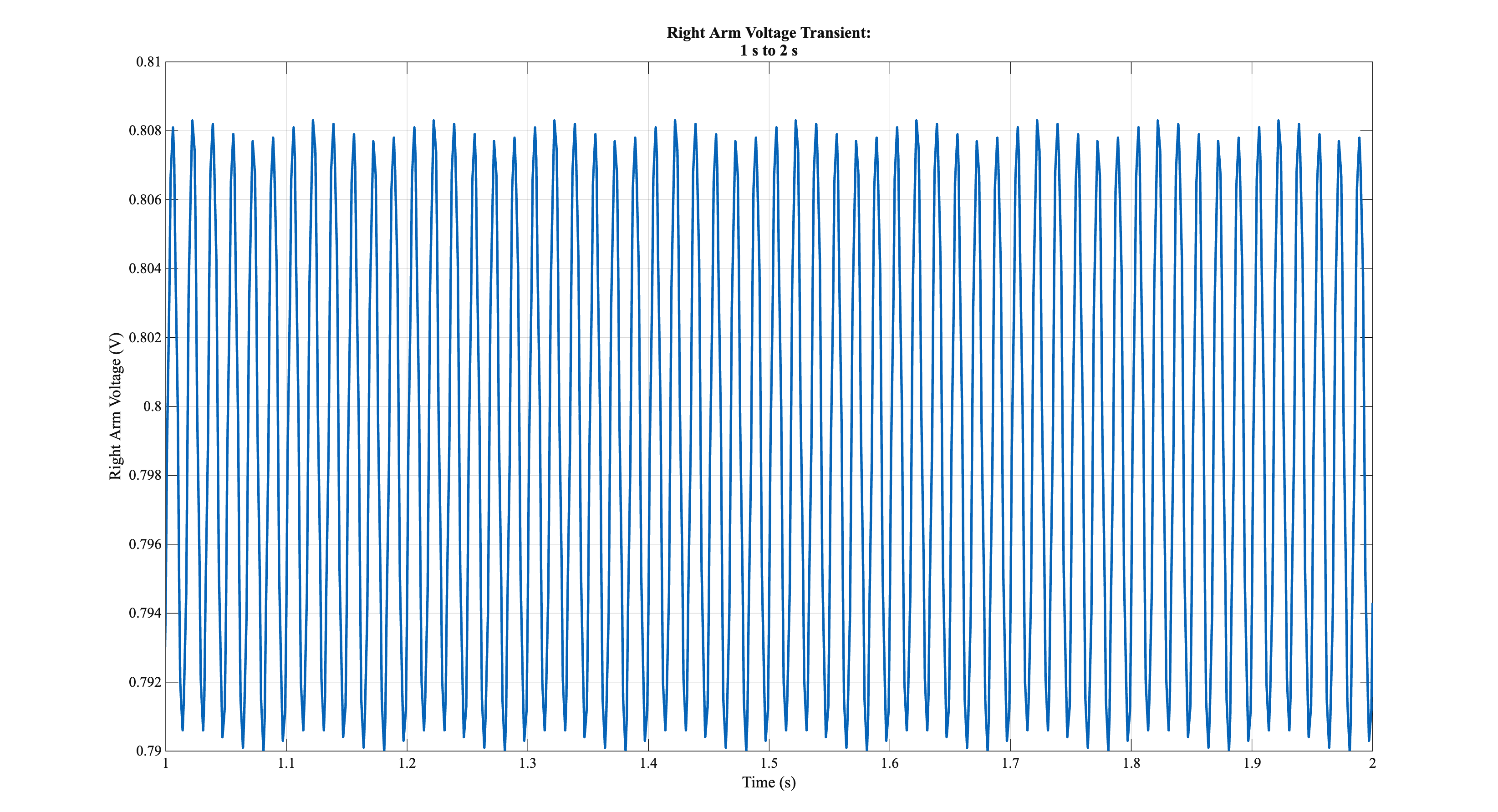
ECG instrumentation amplifier test-bench.
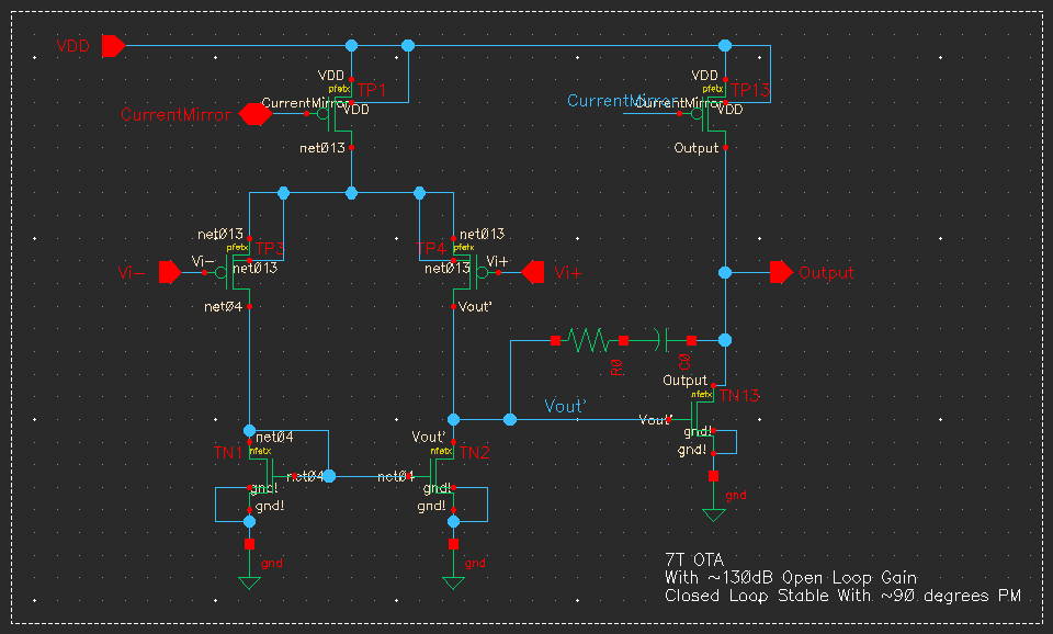
7T OTA op-amp used for the instrumentation amplifier.
5T OTA op-amp used for the DRL driver amplifier.
Human body model.
Monte Carlo simulation of ECG performance.
Right arm transient voltage after the electrodes, before the instrumentation amplifier.
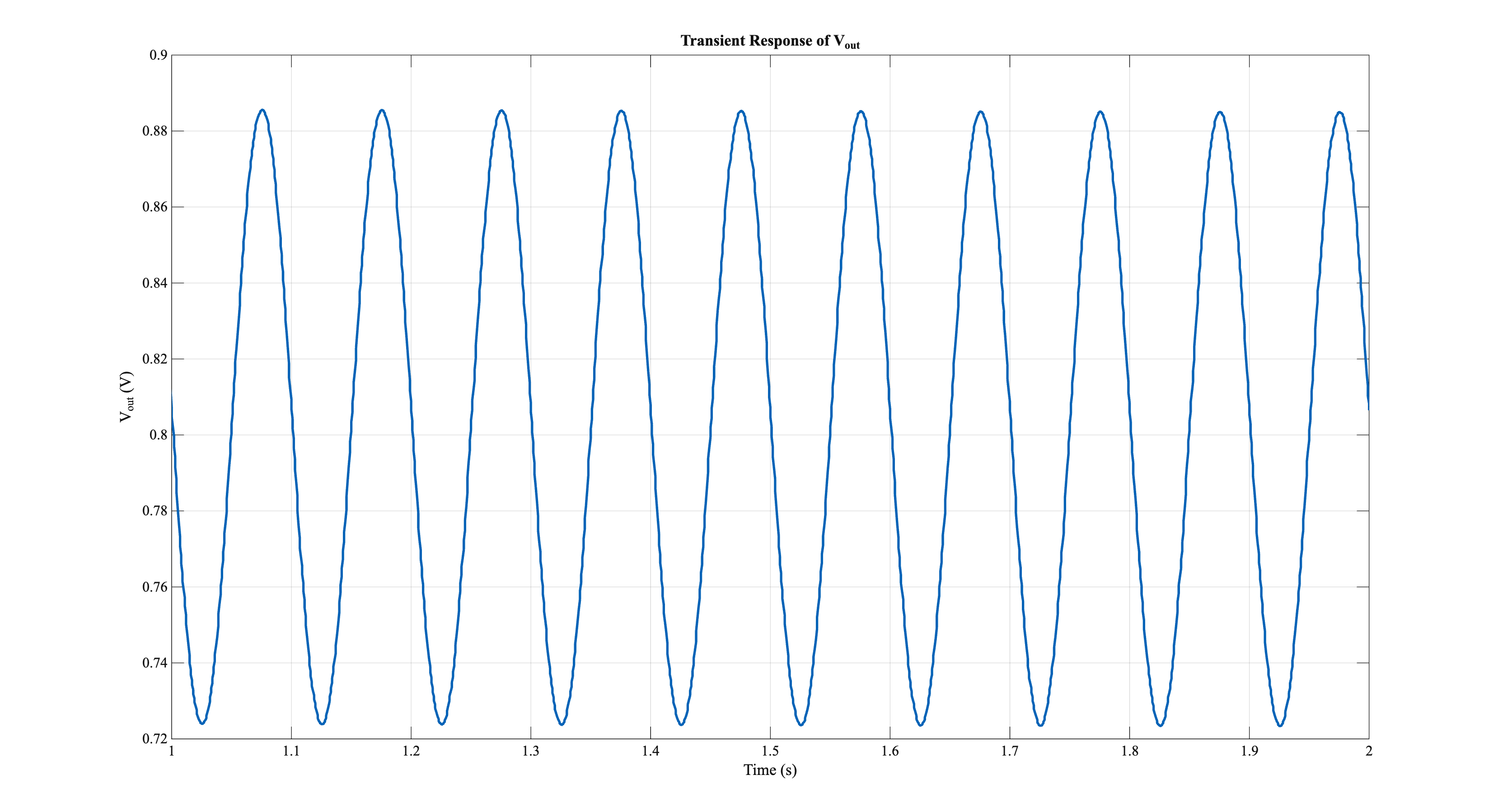
Output of the instrumentation amplifier.
Below is the performance summary of the ECG amplifier in the nominal corner.
| Parameter | Specification | Nominal Performance |
|---|---|---|
| Bandwidth | ~ 100 mHz – 250 Hz | 100.4 mHz – 250.9 Hz |
| Mid-Band Gain | 40 ± 2 dB | 41.443 dB |
| 100 mHz Gain | 37 ± 2 dB | 38.4266 dB |
| Total Integrated Input-Referred Noise | < 3 µVrms | 2.698 µVrms |
| Input Impedance @10 Hz | > 100 MΩ | 1.4578 GΩ |
| Power Consumption | < 4 µW | 667.8 nW !! |
| CMRR w/ DRL @60 Hz | > 85 dB | 125.7 dB |
| CMRR w/o DRL @60 Hz | > 85 dB | 99.3 dB |
| Loop Gain Phase Margin | Closed Loop Stable | 83.01° |
| DRL Loop Gain @60 Hz | Preferably > 20 dB | 25.93 dB |
| NEF | Respectable | 3.897 |
Integrated circuit project
Folded-Cascode OTA
For more information, feel free to read my report.
The following Op-Amp design was assigned as a final project for the upper divisional course ECE164, taught by Professor Drew Hall. For this project, everyone is given the same Op-Amp design, but the sizings are entirely determined by the students.
In this project, my partner and I elected to approach the sizings with a gm/ID approach much akin to the one taught in the textbook "The gm/ID Methodology, a sizing tool for low-voltage analog CMOS Circuits" taught by Professors Paul Jespers and Boris Murmann (Murmann actually gave a seminar on this recently! You can even find the video on youtube!).
Although the design methodology of gm/ID can be applied in many different ways, here is how we used it for this project:
- First choose a general, but well informed, value of gm/ID for your transistor. As an example, a gm/ID of 13 for our input pair devices was the best value possible given the minimum overdrive voltage constraint. This allows us to maximize our gain while also enabling our design to be fast enough to meet the bandwidth specs.
- From here, we used a "square-law" approximation script in matlab to determine the approximate transconductance for a chosen value for gm/ID. This naturally instantly gives us the current, which we can then find the sizings for using provided Id/W look-up tables.
- A similar approach can be used to solve for sizings based off of an expecation for current. As an example, the telescopic stage is not the primary contributor to the dominant and non-dominant poles, and thus it is in our best interest to have less current across them for the sake of intrinsic gain. A similar approach to 2. can now be approached to solve for ro using gm/ro look-up tables and a specificed value for current.
Using our gm/ID approach, we were able to have a great starting point for our circuit. From there a lot of iterative optimization is done to push the overal current down while still meeting spec.
Our design performed so well, we actually got chosen to present to Apple Cohorts during an end of the quarter competition! Unfortunately, out of the four groups that got selected to present, we placed fourth LOL. Shit happens. Still incredibly proud of what we've were able to accomplish, nonetheless!
Here's a summary of our op-amps performance!
| Parameter | Requirement | Our Design |
|---|---|---|
| DC Small-Signal Gain | ≥ 70 dB | 88.36 dB |
| Unity Gain Bandwidth | ≥ 30 MHz | 34.31 MHz |
| Phase Margin | ≥ 65° | 65.45° |
| Gain Margin | ≥ 5 dB | 19.37 dB |
| Input Common Mode Range | 0.2 – 0.8 V | −0.55 – 1.11 V |
| Output Common Mode Range | 0.4 – 1.4 V | 0.21 – 1.65 V |
| Total Power Dissipation | ≤ 2.5 mW | 65.3 µW - The second lowest in the class! |
| Minimum VOV | 150 mV | 152.2 mV |
Integrated circuit project
8-Bit Carry-Less Adder
For more information, feel free to read my report.
I will finish the writeup for this soon!